Tuesday, December 3, 2024

Exploring Innovations in Wafer Susceptor Technology

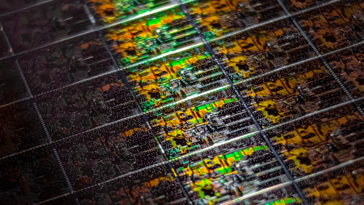
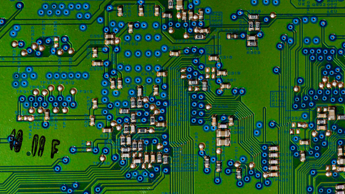
 Wafer susceptor technology plays a pivotal role in semiconductor manufacturing. It ensures precise thermal management, enabling uniform heat distribution during critical processes. Innovations in this field address challenges such as improving efficiency and achieving higher precision in production. The demand for advanced wafer susceptors continues to rise due to trends like miniaturization and the adoption of 3D chip architectures. These advancements drive the industry toward creating smaller, faster, and more reliable electronic devices.

Key Takeaways

  • Wafer susceptors are essential for precise thermal management in semiconductor manufacturing, ensuring uniform heat distribution for high-quality production.
  • Innovations in materials, such as advanced ceramics and specialized coatings, enhance the durability and performance of wafer susceptors, leading to longer lifespans and reduced contamination risks.
  • Design improvements and the integration of sensors allow for real-time monitoring, optimizing manufacturing processes and ensuring consistent quality in semiconductor devices.
  • The competitive landscape is shaped by major players investing in R&D, while startups introduce disruptive technologies that challenge traditional methods and enhance efficiency.
  • Collaboration between semiconductor manufacturers and material science companies drives innovation, resulting in advanced solutions that meet the evolving demands of the industry.
  • Future advancements will likely focus on developing new materials and manufacturing techniques, ensuring wafer susceptors continue to support the production of next-generation electronic devices.

Recent Advancements in Wafer Susceptor Technology

Recent Advancements in Wafer Susceptor Technology

Innovations in Materials

Advancements in materials have significantly improved the performance of wafer susceptors. Manufacturers now utilize advanced ceramics and composite materials to enhance thermal conductivity and durability. These materials withstand extreme temperatures, ensuring consistent performance during high-temperature semiconductor processes. Their robustness reduces wear and tear, extending the lifespan of the susceptor.

Specialized coatings have also emerged as a critical innovation. These coatings improve chemical resistance, protecting the susceptor from corrosive environments. They minimize contamination risks, which is essential for maintaining the purity of wafers during manufacturing. By reducing particle generation, these coatings contribute to higher yields and better-quality semiconductor devices.

Design and Functional Enhancements

Design improvements have optimized the functionality of wafer susceptors. Engineers have developed geometries that ensure uniform heat distribution across the wafer surface. This uniformity eliminates temperature variations, which can lead to defects in semiconductor layers. The precise control of heat enhances the reliability of the manufacturing process.

The integration of sensors represents another breakthrough. These sensors enable real-time monitoring of temperature and other critical parameters. By providing instant feedback, they allow manufacturers to optimize processes and maintain consistent quality. This innovation supports the production of increasingly complex semiconductor devices with tighter tolerances.

Applications in Semiconductor Processes

Wafer susceptors play a vital role in advanced semiconductor processes. In atomic layer deposition (ALD) and epitaxy, they ensure precise thermal control, which is crucial for creating ultra-thin and uniform layers. These processes demand high accuracy, and wafer susceptors meet these requirements by delivering stable and consistent performance.

Their contributions extend to the production of next-generation chips and devices. As the industry moves toward smaller and more powerful components, wafer susceptors enable the fabrication of intricate structures. They support the development of 3D chip architectures and other cutting-edge technologies, driving innovation in electronics.

Key Areas of Innovation

Recent patents highlight significant advancements in wafer susceptor technology. Material innovations have taken center stage, with researchers focusing on improving thermal stability and chemical resistance. These advancements ensure that susceptors perform reliably under extreme conditions, which is critical for semiconductor manufacturing. Process integration has also emerged as a key area of innovation. Patents now emphasize the seamless incorporation of susceptors into advanced manufacturing systems, enhancing efficiency and precision.

One notable example is patent US20060065196A1. This patent introduces a susceptor designed to homogenize the epitaxial layer of a wafer. By ensuring uniformity, it addresses a major challenge in wafer processing. Such innovations not only improve production quality but also reduce defects, which is essential for creating next-generation semiconductor devices.

Geographic Distribution of Patents

The global patent landscape for wafer susceptor technology reveals interesting trends. Countries like the United States, Japan, and South Korea lead in patent filings. These nations invest heavily in research and development, driving innovation in the semiconductor industry. Their focus on advanced materials and manufacturing techniques has positioned them as leaders in this field.

Regional trends also shape the market. In Europe, collaborative efforts between research institutions and private companies have resulted in groundbreaking technologies. Meanwhile, Asian countries prioritize high-volume production, leveraging their expertise in scaling up manufacturing processes. These regional dynamics influence the direction of innovation and competition in the global market.

Collaborations and Partnerships

Collaborations play a crucial role in advancing wafer susceptor technology. Semiconductor manufacturers often partner with material science companies to develop cutting-edge solutions. These joint ventures combine expertise from both fields, resulting in products that meet the industry's evolving demands. For instance, partnerships have led to the creation of susceptors with enhanced durability and performance.

Research institutions also contribute significantly to innovation. Universities and laboratories conduct studies that explore new materials and designs. Their findings often serve as the foundation for commercial applications. By fostering collaboration between academia and industry, these institutions help accelerate the development of advanced wafer susceptor technologies.

Competitive Analysis of the Wafer Susceptor Market

Competitive Analysis of the Wafer Susceptor Market

Major Players and Their Strategies

Key companies dominate the wafer susceptor market by leveraging extensive research and development (R&D) investments. Showa Denko, a prominent player, allocates significant resources to innovate and refine its product offerings. This focus on R&D enables the company to maintain a competitive edge by introducing advanced susceptors with improved performance and durability.

Market leaders adopt strategic approaches to sustain their positions. Acquisitions allow these companies to expand their technological capabilities and market reach. Partnerships with material science firms and semiconductor manufacturers further enhance their ability to meet evolving industry demands. These collaborations foster the development of cutting-edge solutions, ensuring that established players remain at the forefront of innovation.

Challenges in the Industry

The wafer susceptor industry faces several challenges that require careful navigation. Balancing cost pressures with the need for high-quality and reliable products remains a critical concern. Manufacturers must optimize production processes to reduce expenses while maintaining the performance standards demanded by semiconductor applications.

Supply chain disruptions and material shortages present additional hurdles. The reliance on specialized materials, such as advanced ceramics and coatings, makes the industry vulnerable to fluctuations in supply. Companies must implement robust strategies to mitigate these risks, ensuring consistent production and delivery of wafer susceptors to their clients.

Emerging Players and Disruptive Technologies

Startups are entering the wafer susceptor market with innovative designs and materials. These emerging players challenge established companies by introducing novel solutions that address specific industry pain points. Their contributions often focus on enhancing thermal conductivity, chemical resistance, and overall efficiency.

Disruptive technologies have the potential to reshape the competitive landscape. Advanced manufacturing techniques, such as additive manufacturing, enable the creation of complex susceptor geometries with unprecedented precision. These innovations could disrupt traditional production methods, forcing established players to adapt or risk losing market share. The impact of these technologies underscores the importance of continuous innovation in maintaining a competitive advantage.


Innovations in wafer susceptor technology have transformed semiconductor manufacturing by enhancing efficiency, precision, and scalability. These advancements enable the production of smaller, faster, and more reliable electronic devices. The evolving patent landscape highlights the competitive nature of this field, with key players leveraging intellectual property to drive innovation and collaboration. Future breakthroughs will likely focus on advanced materials, improved designs, and disruptive manufacturing techniques. As the industry progresses, wafer susceptors will remain critical to meeting the demands of next-generation semiconductor technologies.

FAQ

What is a wafer susceptor?

A wafer susceptor is a critical component in semiconductor manufacturing. It holds and supports wafers during processes like chemical vapor deposition (CVD) and epitaxy. Its primary function involves ensuring uniform heat distribution and maintaining precise thermal control to achieve high-quality semiconductor layers.

Why are advanced materials important for wafer susceptors?

Advanced materials enhance the performance and durability of wafer susceptors. Materials like ceramics and composites improve thermal conductivity and withstand extreme temperatures. These properties ensure consistent performance, reduce wear and tear, and extend the lifespan of the susceptor.

How do specialized coatings benefit wafer susceptors?

Specialized coatings provide chemical resistance and minimize contamination risks. They protect susceptors from corrosive environments and reduce particle generation. This ensures wafer purity, leading to higher yields and better-quality semiconductor devices.

What role do sensors play in wafer susceptor technology?

Sensors integrated into wafer susceptors enable real-time monitoring of critical parameters like temperature. They provide instant feedback, allowing manufacturers to optimize processes and maintain consistent quality. This innovation supports the production of complex semiconductor devices with tighter tolerances.

How do wafer susceptors contribute to advanced semiconductor processes?

Wafer susceptors ensure precise thermal control in processes like atomic layer deposition (ALD) and epitaxy. These processes require high accuracy to create ultra-thin and uniform layers. Susceptors play a vital role in achieving the precision needed for next-generation chips and devices.

Which companies lead the wafer susceptor market?

Major players like Showa Denko dominate the wafer susceptor market. These companies invest heavily in research and development to introduce advanced susceptors. Their strategies include acquisitions and partnerships to maintain market leadership and meet evolving industry demands.

What challenges does the wafer susceptor industry face?

The industry faces challenges such as balancing cost pressures with quality requirements. Supply chain disruptions and material shortages also pose significant hurdles. Manufacturers must adopt strategies to mitigate these risks and ensure consistent production.

How are startups influencing wafer susceptor technology?

Startups bring innovative designs and materials to the wafer susceptor market. They address specific industry pain points by introducing solutions that enhance thermal conductivity, chemical resistance, and efficiency. These emerging players challenge established companies and drive competition.

What are some notable patents in wafer susceptor technology?

Patent US20060065196A1 stands out for its contribution to wafer processing. It introduces a susceptor designed to homogenize the epitaxial layer of a wafer, addressing a major challenge in semiconductor manufacturing. Such patents highlight advancements in material and process integration.

Future trends focus on advanced materials, improved designs, and disruptive manufacturing techniques like additive manufacturing. These innovations aim to enhance efficiency, precision, and scalability. The evolving patent landscape and collaborations will continue to drive progress in this field.

Best Practices for Using Silicon Epitaxy Carriers in MOCVD


Best Practices for Using Silicon Epitaxy Carriers in MOCVD

Silicon epitaxy carriers play a pivotal role in achieving precise and high-quality epitaxial growth. These carriers ensure uniform thermal distribution, which directly impacts the efficiency and consistency of the MOCVD process. By optimizing thermal management, they help you enhance yield and reduce defects in the final product. Proper handling and usage of these carriers prevent contamination and ensure stable growth conditions. Their design and material properties contribute significantly to maintaining process reliability, making them indispensable for achieving superior results in epitaxial layer production.

Key Takeaways

  • Silicon epitaxy carriers are essential for achieving uniform thermal distribution, which enhances the quality and efficiency of the MOCVD process.
  • Choosing the right carrier material, such as silicon carbide or graphite, is crucial for compatibility with substrates and process requirements.
  • Regular cleaning and inspection of carriers prevent contamination and extend their lifespan, ensuring consistent epitaxial growth.
  • Utilizing rotating carriers can significantly improve gas distribution and deposition uniformity, leading to higher quality epitaxial layers.
  • Monitoring for signs of wear and damage allows for timely repairs or replacements, maintaining optimal performance in MOCVD processes.
  • Customizing carrier designs to fit specific applications can enhance process efficiency and reliability, addressing unique growth needs.

Overview of Silicon Epitaxy Carriers

Overview of Silicon Epitaxy Carriers

What Are Silicon Epitaxy Carriers?

Definition and purpose in MOCVD processes

A silicon epitaxy carrier serves as a critical component in the Metal-Organic Chemical Vapor Deposition (MOCVD) process. It holds the substrate securely during epitaxial growth, ensuring precise positioning and stability. This carrier facilitates uniform deposition of thin films by maintaining consistent thermal and chemical conditions. Its role directly impacts the quality of the epitaxial layers, making it indispensable for achieving high-performance semiconductor devices.

The primary purpose of a silicon epitaxy carrier is to optimize the growth environment. It ensures that substrates experience uniform temperature distribution and controlled gas flow. These factors are essential for producing defect-free epitaxial layers with consistent thickness and composition. By using a well-designed carrier, you can enhance the efficiency and reliability of your MOCVD process.

Key features and materials used in their construction

Silicon epitaxy carriers are designed with specific features to meet the demands of MOCVD processes. High thermal conductivity is one of the most important characteristics. This property ensures that heat distributes evenly across the substrate, preventing localized overheating or cooling. Durability is another key feature, as carriers must withstand extreme temperatures and corrosive environments without degrading.

The materials used in constructing these carriers vary based on application requirements. Common options include graphite and silicon carbide coatings. Graphite offers excellent thermal stability and machinability, making it a popular choice. Silicon carbide coatings enhance the carrier's resistance to wear and chemical attack, extending its lifespan. By selecting the right material, you can ensure compatibility with your process and improve overall performance.

Types of Silicon Epitaxy Carriers

Fixed carriers vs. rotating carriers

Silicon epitaxy carriers come in two main types: fixed and rotating. Fixed carriers remain stationary during the MOCVD process. They are ideal for applications requiring precise control over gas flow and deposition patterns. These carriers provide stability, which helps maintain uniformity in epitaxial growth.

Rotating carriers, on the other hand, spin during the deposition process. This rotation promotes even gas distribution and enhances film uniformity. It also reduces the risk of defects caused by uneven deposition. Rotating carriers are particularly useful for large-scale production, where consistency across multiple substrates is critical. Choosing between fixed and rotating carriers depends on your specific process requirements and desired outcomes.

Material variations (e.g., graphite, silicon carbide coatings)

Material selection plays a vital role in the performance of silicon epitaxy carriers. Graphite carriers are lightweight and thermally stable, making them suitable for high-temperature applications. They are also easy to machine, allowing for customization to fit unique process needs. However, graphite can be prone to wear over time, especially in harsh chemical environments.

Silicon carbide-coated carriers offer enhanced durability and chemical resistance. The coating protects the underlying material from corrosion and mechanical damage, extending the carrier's operational life. This option is ideal for processes involving aggressive chemicals or prolonged high-temperature exposure. By understanding the strengths and limitations of each material, you can select the best carrier for your MOCVD system.

Key Considerations for Using Silicon Epitaxy Carriers

Material Compatibility

Importance of matching carrier material with substrate and process requirements

Selecting the right material for your silicon epitaxy carrier is crucial for achieving optimal results in MOCVD processes. The carrier material must align with the substrate's properties and the specific requirements of your process. For example, if you work with high-temperature applications, a carrier with excellent thermal stability, such as silicon carbide-coated graphite, ensures reliable performance. Matching the carrier material to your substrate minimizes the risk of thermal mismatch, which can lead to defects or uneven growth.

When you choose a compatible carrier material, you also enhance the overall efficiency of your process. Proper material selection ensures that the carrier supports uniform deposition and maintains the integrity of the epitaxial layers. This alignment between carrier and substrate creates a stable environment for consistent growth, reducing variability and improving yield.

Avoiding contamination and ensuring chemical stability

Contamination poses a significant threat to the quality of epitaxial layers. To prevent this, you must ensure that the carrier material resists chemical reactions during the MOCVD process. Materials like silicon carbide coatings provide excellent chemical stability, protecting the carrier from reacting with precursors or byproducts. This stability reduces the risk of introducing impurities into the growth environment.

Regular cleaning and inspection of carriers also play a vital role in avoiding contamination. Residual particles or chemical buildup on the carrier surface can compromise the quality of subsequent runs. By maintaining a clean and stable carrier, you safeguard the purity of your epitaxial layers and maintain consistent process conditions.

Thermal Stability and Uniformity

Ensuring carriers can withstand high temperatures without deformation

MOCVD processes often involve extreme temperatures, making thermal stability a critical factor for silicon epitaxy carriers. Your carrier must endure these conditions without warping or degrading. Materials like graphite and silicon carbide are designed to handle high temperatures while maintaining their structural integrity. A carrier that deforms under heat can disrupt substrate positioning, leading to uneven deposition and defects.

Thermal stability also ensures that the carrier remains reusable over multiple cycles. A durable carrier reduces the need for frequent replacements, saving time and costs. By investing in a thermally stable carrier, you enhance the reliability and longevity of your MOCVD system.

Role of thermal uniformity in achieving consistent epitaxial layers

Thermal uniformity directly impacts the quality of epitaxial growth. A silicon epitaxy carrier must distribute heat evenly across the substrate to prevent localized temperature variations. Uneven heating can cause non-uniform deposition, resulting in inconsistent layer thickness or composition. Carriers with high thermal conductivity, such as those made from silicon carbide-coated materials, excel at maintaining uniform temperatures.

To achieve consistent epitaxial layers, you should monitor the carrier's performance during the process. Advanced carrier designs often incorporate features that enhance thermal uniformity, such as optimized geometries or coatings. By prioritizing thermal uniformity, you ensure that your substrates experience stable growth conditions, leading to superior results.

Carrier Design and Geometry

Impact of carrier design on gas flow and deposition uniformity

The design of your silicon epitaxy carrier significantly influences gas flow dynamics within the reactor. A well-designed carrier promotes even distribution of precursor gases across the substrate surface. This uniform gas flow ensures consistent deposition rates, reducing the likelihood of defects or irregularities in the epitaxial layers.

Carriers with optimized geometries enhance the overall efficiency of the MOCVD process. For instance, designs that minimize turbulence or dead zones improve gas utilization and deposition precision. By selecting a carrier with an appropriate design, you can achieve better control over your process and enhance the quality of your output.

Customization options for specific MOCVD applications

Every MOCVD application has unique requirements, and carrier customization allows you to address these needs effectively. Custom carriers can be tailored to accommodate specific substrate sizes, shapes, or orientations. They can also include features that optimize thermal or chemical performance for your particular process.

Working with manufacturers to design a carrier that aligns with your goals can yield significant benefits. Customization ensures that the carrier integrates seamlessly into your system, enhancing both efficiency and reliability. By leveraging tailored solutions, you can maximize the potential of your MOCVD process and achieve superior results.

Best Practices for MOCVD Growth

Best Practices for MOCVD Growth

Preparing Silicon Epitaxy Carriers

Cleaning and pre-treatment steps to prevent contamination

Proper cleaning and pre-treatment of your silicon epitaxy carrier are essential for maintaining a contamination-free environment. Residual particles, oils, or chemical residues on the carrier surface can compromise the quality of epitaxial growth. To prevent this, you should implement a thorough cleaning protocol before each use.

Start by using a non-abrasive cleaning solution that effectively removes contaminants without damaging the carrier material. Ultrasonic cleaning systems can enhance this process by dislodging microscopic particles from hard-to-reach areas. After cleaning, rinse the carrier with deionized water to eliminate any remaining residues. Dry the carrier completely in a cleanroom environment to avoid introducing airborne particles.

Pre-treatment steps, such as surface conditioning, can further optimize the carrier for MOCVD processes. Conditioning ensures that the carrier surface is chemically stable and ready to support uniform deposition. By prioritizing these steps, you create a controlled environment that minimizes defects and enhances growth consistency.

Inspecting carriers for damage or wear before use

Before using a silicon epitaxy carrier, inspect it for signs of damage or wear. Cracks, chips, or surface irregularities can disrupt substrate positioning and lead to uneven deposition. Examine the carrier under proper lighting to identify any visible defects. Pay close attention to edges and corners, as these areas are more prone to damage.

For carriers with coatings, such as silicon carbide, check for signs of wear or peeling. A compromised coating can expose the underlying material to chemical reactions, increasing the risk of contamination. If you detect any issues, replace or repair the carrier to maintain optimal performance. Regular inspections ensure that your carrier remains reliable and contributes to consistent epitaxial growth.

Maintenance and Longevity

Regular cleaning protocols to extend carrier lifespan

Establishing a regular cleaning routine is crucial for extending the lifespan of your silicon epitaxy carrier. Over time, deposits from precursors and byproducts can accumulate on the carrier surface, affecting its performance. Frequent cleaning prevents buildup and ensures that the carrier continues to function effectively.

Use cleaning methods that align with the carrier's material properties. For example, carriers with silicon carbide coatings require gentle cleaning solutions to avoid damaging the protective layer. Avoid abrasive tools or harsh chemicals that could degrade the carrier. By maintaining a consistent cleaning schedule, you reduce wear and prolong the carrier's usability.

Monitoring for signs of degradation or coating wear

Monitoring the condition of your silicon epitaxy carrier helps you identify early signs of degradation. Regularly assess the carrier for structural integrity and coating stability. Look for discoloration, surface roughness, or other indicators of wear. These signs suggest that the carrier may no longer provide optimal thermal or chemical performance.

Document your observations to track the carrier's condition over time. This practice allows you to predict when replacements or repairs may be necessary. Proactive monitoring ensures that your carrier remains in peak condition, supporting efficient and reliable MOCVD processes.

Process Optimization Techniques

Adjusting process parameters for carrier-specific performance

Optimizing your MOCVD process involves tailoring parameters to the specific characteristics of your silicon epitaxy carrier. Factors such as carrier material, design, and thermal conductivity influence how the carrier interacts with the process environment. Adjusting parameters like temperature, gas flow, and pressure ensures that the carrier performs at its best.

For instance, carriers with high thermal conductivity may require lower temperature gradients to maintain uniform deposition. Experiment with different settings to identify the optimal configuration for your carrier. By fine-tuning these parameters, you enhance the quality and consistency of your epitaxial layers.

Leveraging carrier rotation for improved uniformity

Rotating carriers offer a practical solution for achieving uniform deposition across substrates. The rotation promotes even distribution of precursor gases, reducing the risk of localized variations in film thickness or composition. If your MOCVD system supports carrier rotation, take advantage of this feature to enhance growth uniformity.

Monitor the rotation speed to ensure it aligns with your process requirements. Excessive speeds can introduce turbulence, while insufficient speeds may not provide adequate gas distribution. By leveraging carrier rotation effectively, you improve the overall quality of your epitaxial layers and maximize process efficiency.

Common Challenges and Solutions

Contamination Issues

Sources of contamination and their impact on epitaxial growth

Contamination remains one of the most critical challenges in achieving high-quality epitaxial growth. It can originate from multiple sources, including residual particles on the silicon epitaxy carrier, impurities in the precursor gases, or even airborne contaminants in the reactor environment. These impurities can deposit onto the substrate during the MOCVD process, leading to defects such as dislocations, pits, or uneven film thickness.

Contaminants disrupt the chemical reactions necessary for uniform epitaxial layer formation. For example, metallic particles can act as nucleation sites, causing unwanted growth patterns. Organic residues may decompose at high temperatures, introducing carbon impurities into the layer. These issues compromise the electrical and structural properties of the epitaxial layers, reducing the performance and reliability of the final semiconductor device.

Strategies for preventing and mitigating contamination

You can implement several strategies to minimize contamination risks. Start by ensuring that your silicon epitaxy carriers undergo thorough cleaning before each use. Use non-abrasive cleaning agents and advanced techniques like ultrasonic cleaning to remove microscopic particles and residues. Always dry the carriers in a cleanroom environment to prevent recontamination.

Maintain strict control over the reactor environment. Regularly inspect and replace filters in the gas delivery system to ensure the purity of precursor gases. Monitor the reactor chamber for signs of particle buildup or chemical deposits, and schedule periodic maintenance to keep it in optimal condition.

Adopt proper handling protocols for carriers and substrates. Use clean gloves and tools to avoid transferring oils or particles. Store carriers in sealed containers when not in use to protect them from airborne contaminants. By following these practices, you can create a controlled environment that supports defect-free epitaxial growth.

Carrier Degradation

Causes of wear and damage in silicon epitaxy carriers

Silicon epitaxy carriers face significant wear and damage over time due to the harsh conditions of the MOCVD process. High temperatures, chemical exposure, and mechanical stress contribute to their degradation. Thermal cycling during repeated heating and cooling can cause materials like graphite to develop cracks or lose structural integrity. Prolonged exposure to corrosive precursors may erode protective coatings, such as silicon carbide, leaving the underlying material vulnerable.

Improper handling also accelerates carrier wear. Dropping or mishandling carriers can result in chips, scratches, or other physical damage. Even minor surface irregularities can disrupt substrate positioning, leading to uneven deposition and defects in the epitaxial layers.

Repair and replacement guidelines

Regular inspection helps you identify early signs of carrier degradation. Look for visible cracks, discoloration, or peeling coatings. If you detect minor damage, consider repairing the carrier. For example, reapplying a silicon carbide coating can restore its chemical resistance and thermal stability. Consult with manufacturers or service providers for professional repair options.

When damage becomes extensive, replace the carrier to maintain process reliability. Using a degraded carrier increases the risk of contamination and inconsistent growth results. Keep spare carriers on hand to minimize downtime during replacements. By proactively addressing wear and damage, you ensure that your carriers continue to support efficient and high-quality MOCVD processes.

Process Variability

Factors contributing to inconsistent growth results

Process variability arises from several factors, including fluctuations in temperature, gas flow, and pressure within the reactor. Even slight deviations in these parameters can lead to non-uniform deposition, resulting in variations in layer thickness, composition, or crystal quality. Misalignment of the silicon epitaxy carrier or substrate can further exacerbate these inconsistencies.

Material inconsistencies in the carrier itself also contribute to variability. For instance, uneven thermal conductivity across the carrier surface may cause localized temperature differences, affecting the growth rate. Additionally, worn or damaged carriers may fail to provide the stable environment needed for consistent epitaxial growth.

Techniques for stabilizing process conditions

To stabilize process conditions, start by calibrating your MOCVD system regularly. Verify that temperature sensors, gas flow controllers, and pressure regulators function accurately. Use advanced monitoring systems to track these parameters in real time and make adjustments as needed.

Ensure proper alignment of the silicon epitaxy carrier and substrate within the reactor. Use carriers with precise geometries and high thermal conductivity to promote uniform temperature distribution. If your process involves rotating carriers, optimize the rotation speed to enhance gas flow and deposition uniformity.

Document your process parameters and results to identify trends or recurring issues. Use this data to refine your settings and improve reproducibility. By implementing these techniques, you can reduce variability and achieve consistent, high-quality epitaxial layers.


Selecting and maintaining high-quality silicon epitaxy carriers is essential for achieving superior results in MOCVD processes. These carriers directly influence the consistency, efficiency, and quality of epitaxial growth. By following best practices, you can optimize preparation, ensure proper maintenance, and fine-tune process parameters for maximum performance.

Focus on:

  • Cleaning and inspecting carriers to prevent contamination.
  • Monitoring for wear to extend carrier lifespan.
  • Adjusting process settings to match carrier-specific needs.

Implementing these strategies will enhance your growth quality, improve yields, and boost overall efficiency. Take action today to elevate your MOCVD outcomes and maintain a competitive edge.

FAQ

What is the primary purpose of silicon epitaxy carriers in MOCVD?

Silicon epitaxy carriers ensure precise substrate positioning and stable conditions during epitaxial growth. They optimize thermal distribution and gas flow, which are critical for achieving uniform and defect-free layers. By using these carriers, you can enhance the efficiency and reliability of your MOCVD process.

How do I choose the right material for my silicon epitaxy carrier?

For high-temperature applications, silicon carbide-coated carriers offer excellent thermal stability and chemical resistance.

Why is cleaning silicon epitaxy carriers important?

Cleaning removes contaminants like particles, oils, and residues that can compromise epitaxial growth. A clean carrier ensures a pure environment, reducing the risk of defects in the layers. Regular cleaning also extends the carrier's lifespan by preventing buildup that could degrade its performance.

How often should I inspect my silicon epitaxy carriers?

Inspect your carriers before every use. Look for visible damage, such as cracks, chips, or coating wear. Regular inspections help you identify issues early, allowing you to repair or replace carriers before they affect your process. Consistent monitoring ensures reliable performance and high-quality results.

What are the benefits of rotating carriers in MOCVD?

Rotating carriers improve gas distribution and promote uniform deposition across the substrate. This reduces the risk of localized defects and enhances layer consistency. If your system supports rotation, you can achieve better uniformity and higher yields by leveraging this feature.

How can I prevent contamination during the MOCVD process?

To prevent contamination, clean your carriers thoroughly before each use. Use high-purity precursor gases and maintain a clean reactor environment. Handle carriers with clean gloves and store them in sealed containers when not in use. These practices help you maintain a controlled environment for defect-free growth.

What should I do if my carrier shows signs of wear or damage?

If you notice minor wear, consider repairing the carrier. For example, reapplying a silicon carbide coating can restore its protective properties. Replace carriers with extensive damage to avoid process disruptions. Keeping spare carriers on hand ensures minimal downtime during replacements.

How does carrier design impact the MOCVD process?

Carrier design affects gas flow dynamics and deposition uniformity. A well-designed carrier promotes even gas distribution, reducing defects and improving layer quality. Custom designs tailored to your specific application can further enhance process efficiency and reliability.

Can I customize silicon epitaxy carriers for my specific needs?

Yes, you can customize carriers to fit your unique requirements. Customization options include specific sizes, shapes, and features that optimize thermal or chemical performance. Working with manufacturers to design tailored carriers ensures seamless integration into your MOCVD system.

What are the key steps to extend the lifespan of silicon epitaxy carriers?

To extend carrier lifespan, follow a regular cleaning routine using non-abrasive methods. Inspect carriers frequently for signs of wear or damage. Handle carriers carefully to avoid physical damage. By maintaining proper care, you can maximize the durability and performance of your carriers.

How Silicon Carbide Coating on Graphite Components Advances Technology in 2025

  You might not realize it, but silicon carbide coating on graphite components is shaping the future of advanced technologies in 2025. Thi...