Semicera Semiconductor integrates R&D and production with dual research centers and three production bases, supporting 50 production lines and 200+ employees.
In
the era of rapid development of materials science, silicon carbide
coating has become the focus of attention in many fields due to its
unique properties. This coating material not only excels in enhancing
product performance but also plays a crucial role in promoting
technological innovation across various industries. This article will
delve into the characteristics, application areas, and market prospects
of silicon carbide coating. Additionally, it will introduce Semicera
Semiconductor, a company deeply rooted in this field, boasting strong R
& D and production capabilities.
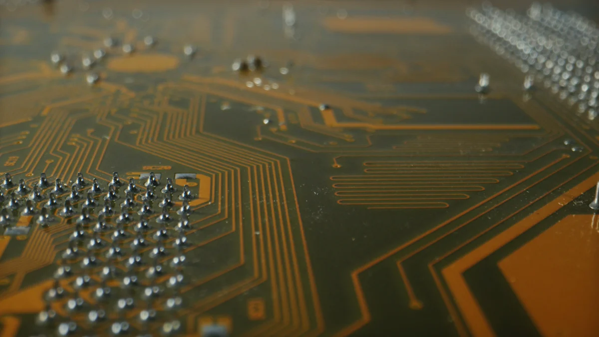
2. Understanding Silicon Carbide Coating
2.1 Definition and Composition
Silicon carbide coating is mainly composed of silicon (Si) and carbon (C)
elements. Its unique molecular structure endows it with distinctive
properties. In the crystal structure of silicon carbide, silicon atoms
and carbon atoms are closely connected by covalent bonds, forming a
stable and ordered lattice structure. This structure not only determines
the basic physical and chemical properties of the silicon carbide
coating but also serves as the inherent source of its outstanding
performance.
2.2 Preparation Processes
Chemical Vapor Deposition (CVD): This is a commonly
used method for preparing silicon carbide coatings. Gaseous reactants
containing silicon and carbon sources are decomposed under high -
temperature and specific chemical reaction conditions and then deposited
on the surface of the substrate material, forming a uniform and dense
silicon carbide coating. The coating prepared by CVD has good purity and
consistency, allowing for precise control of the coating thickness and
microstructure. It is suitable for applications with high requirements
for coating quality, such as semiconductor device manufacturing.
Physical Vapor Deposition (PVD): In a high - vacuum
environment, this method evaporates or sputters the silicon and carbon
source materials through physical means, causing them to condense on the
substrate surface to form a coating. The silicon carbide coating
prepared by PVD has a strong adhesion to the substrate and a relatively
fast deposition rate. It can be used to prepare components with high
requirements for coating adhesion and deposition efficiency.
Thermal Spraying: The silicon carbide powder is
heated to a molten or semi - molten state and then sprayed onto the
surface of the substrate material through a high - speed gas flow to
form a coating. The thermal spraying process is relatively simple and
can quickly prepare coatings on large - area substrates. It is often
used in industrial applications where a relatively high coating
thickness is required and the precision of the microstructure is
relatively less critical, such as wear protection of mechanical parts.
3. Deciphering the Outstanding Performance
3.1 Hardness and Wear Resistance
The
high hardness of the silicon carbide coating is one of its remarkable
features. This high hardness stems from the strong covalent bond
interactions within its crystal structure. The high bond energy between
silicon and carbon atoms makes the crystal structure extremely stable
and difficult to be damaged by external forces. On the Mohs hardness
scale, the hardness of the silicon carbide coating is much higher than
that of many common metals and ceramics, second only to super - hard
materials such as diamond. This property makes the silicon carbide
coating outstanding in wear resistance. In practical applications, for
example, in the machining industry, when the surface of a cutting tool
is coated with silicon carbide, its wear resistance is significantly
improved. This can significantly extend the service life of the cutting
tool, reduce the frequency of tool replacement, thereby improving
production efficiency and reducing production costs. Compared with
traditional uncoated cutting tools, the wear rate of cutting tools
coated with silicon carbide coating can be reduced by several times or
even dozens of times under the same cutting conditions.
3.2 High - Temperature Resistance
The
silicon carbide coating exhibits excellent high - temperature
resistance, which benefits from its special bond energy and the
stability of its crystal structure. In a high - temperature environment,
the silicon carbide coating can maintain the integrity of its structure
and the relative stability of its physical and chemical properties.
Generally, the silicon carbide coating can work stably at temperatures
up to 1600 °C or even higher. In the aerospace field, for example, some
key components of engines, such as combustion chambers and turbine
blades, face extremely high temperatures during operation. By coating
with silicon carbide, these components can effectively resist thermal
corrosion and thermal fatigue in a high - temperature environment,
ensuring the reliable operation of the engine and improving the
performance and service life of the aero - engine.
3.3 Chemical Stability
The
silicon carbide coating performs exceptionally well in terms of
chemical stability. Its chemical stability originates from the chemical
inertness of silicon carbide itself and the compactness of the coating
structure. In common chemical corrosion environments, such as acid and
alkali solutions and some corrosive gas atmospheres, the silicon carbide
coating can effectively prevent the contact between the corrosive
medium and the substrate material, thus protecting the substrate
material from erosion. In the chemical industry, many reaction kettles
and pipelines need to operate in harsh chemical environments such as
strong acids and alkalis. The silicon carbide coating can provide
reliable protection for these devices, extend their service life, and
reduce leakage and safety hazards caused by corrosion. Compared with
ordinary metal materials, the corrosion rate of equipment coated with
silicon carbide coating can be reduced to a fraction or even less of the
original in the same corrosive environment.
4. Diverse Application Fields
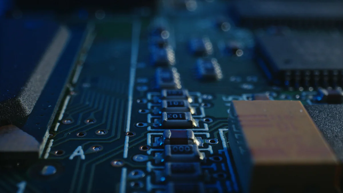
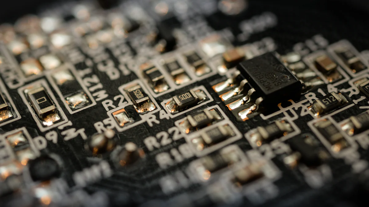
4.1 Electronics and Semiconductor Industry
Silicon carbide coating plays a vital role in the electronics and semiconductor field. With the continuous miniaturization and high - performance
development of semiconductor devices, the requirements for material
properties are becoming increasingly stringent. Due to its high thermal
conductivity, good chemical stability, and compatibility with
semiconductor materials, silicon carbide coating is widely used in the
manufacturing process of semiconductor devices. For example, in the
photolithography process of chip manufacturing, the silicon carbide
coating can be used to make the protective coating of the photomask,
effectively preventing the photomask from being corroded by chemical
reagents and physically damaged during multiple photolithography
processes, thereby improving the photolithography accuracy and the
service life of the photomask. In addition, in power semiconductor
devices, the silicon carbide coating can be used to improve the heat
dissipation performance of the devices, increase the power density and
reliability of the devices, and promote the development of power
electronics technology.
4.2 Machining Field
In
the machining industry, the application of silicon carbide coating has
brought revolutionary changes to the performance of cutting tools and
molds. As mentioned earlier, the high hardness and wear resistance of
the silicon carbide coating enable cutting tools to withstand higher
cutting forces and temperatures during cutting, reducing tool wear and
improving machining accuracy and surface quality. Whether it is high -
speed steel cutting tools or cemented carbide cutting tools, their
cutting performance can be significantly improved after being coated
with silicon carbide. In mold manufacturing, the silicon carbide coating
can improve the demolding performance of the mold, reduce the friction
and adhesion between the mold and the molding material, thereby
improving the service life of the mold and the quality of the molded
products. For example, after coating the injection mold and die -
casting mold with silicon carbide coating, the demolding resistance can
be effectively reduced, and surface defects of products can be
decreased, improving production efficiency and product yield.
4.3 Energy and Environmental Protection Field
Photovoltaic Industry: In the solar photovoltaic
field, silicon carbide coating is mainly applied to the production
equipment of photovoltaic cells and the packaging materials of
photovoltaic modules. During the manufacturing process of photovoltaic
cells, the silicon carbide coating can be used to coat the silicon wafer
cutting tools, improving the cutting efficiency and service life of the
tools and reducing the silicon wafer cutting loss. At the same time,
during the packaging process of photovoltaic modules, the silicon
carbide coating can be used as a high - performance protective coating
to improve the weather resistance and anti - aging performance of the
photovoltaic modules, ensuring the stable operation of the photovoltaic
modules during long - term outdoor use and improving the overall
efficiency and reliability of the photovoltaic power generation system.
Battery Field: With the rapid development of
electric vehicles and energy storage technologies, the requirements for
battery performance are getting higher and higher. The application of
silicon carbide coating in the battery field mainly focuses on the
protection of battery electrode materials and battery casings. Coating
the surface of electrode materials with silicon carbide can improve the
electrical conductivity and stability of the electrode materials,
increasing the charge - discharge efficiency and cycle life of the
battery. At the same time, coating the surface of the battery casing
with silicon carbide can enhance the mechanical strength and corrosion
resistance of the battery casing, improving the safety and reliability
of the battery.
5. Insights into the Market Prospect
5.1 Current Situation Analysis
At
present, the silicon carbide coating market is showing a booming
development trend. With the continuous growth of demand for high -
performance materials in various industries, the market size of silicon
carbide coating is constantly expanding. In terms of geographical
distribution, the Asia - Pacific region has become the largest consumer
market for silicon carbide coatings due to the rapid development of
manufacturing industries such as electronics and machinery. In terms of
industry demand, the electronics and semiconductor, machining, and
energy sectors are the main application industries for silicon carbide
coatings, accounting for a large part of the market share. According to
data from market research institutions, the annual growth rate of the
silicon carbide coating market has remained at around [X]% in the past
few years, and it is expected to maintain a relatively high growth rate
in the next few years.
5.2 Future Outlook
With
the continuous progress of science and technology, the silicon carbide
coating market faces many opportunities and challenges. On the one hand,
the rapid development of emerging technologies such as 5G
communication, artificial intelligence, and new energy vehicles will
further drive the demand for silicon carbide coatings. For example, the
increasing demand for high - performance semiconductor devices in 5G
communication base stations will boost the application of silicon
carbide coatings in semiconductor manufacturing; the booming development
of the new energy vehicle industry will promote the application of
silicon carbide coatings in key components such as batteries and motors.
On the other hand, market competition is becoming increasingly fierce,
posing higher requirements for the performance, quality, and cost
control of silicon carbide coatings. To meet these challenges, companies
need to continuously increase R & D investment, enhance
technological innovation capabilities, optimize production processes,
and reduce production costs to improve the competitiveness of their
products.
6. Semicera Semiconductor: A Leader in the Industry
Semicera
Semiconductor, an outstanding representative in the industry, is a
company integrating R & D and production. The company has two
research centers and three production bases. Its strong hardware
facilities provide a solid guarantee for product innovation and
production. Fifty production lines operate in an orderly manner, and
more than 200 employees work together. More than 25% of the team members
are dedicated to R & D, striving for excellence in various aspects
such as technology, production, sales, and operation management.
The
company's products widely serve important industries such as LED, IC
integrated circuits, third - generation semiconductors, and
photovoltaics. As a leading supplier of advanced semiconductor ceramics,
Semicera Semiconductor provides high - purity silicon carbide (SiC)
ceramics, CVD SiC, and TaC coatings. Its main products include graphite
susceptors coated with SiC, pre - heat rings, and diversion rings coated
with TaC. The purity level of these products is controlled below 5ppm,
which can accurately meet the diverse needs of customers. Whether in
terms of product quality or performance, Semicera Semiconductor has
demonstrated excellent strength, setting a benchmark for the development
of the industry.
7. Conclusion
Silicon
carbide coating occupies an important position in the field of
materials science with its outstanding performance and wide range of
applications. With the continuous technological progress of various
industries, its market prospects are becoming more and more promising.
Companies like Semicera Semiconductor, with strong R & D and
production capabilities, are promoting the development and application
of silicon carbide coating technology through continuous innovation and
product optimization. It is believed that in the future, silicon carbide
coating will play an important role in more fields, injecting new
vitality into the development of various industries.
Epitaxy serves as a cornerstone in modern electronics, enabling the creation of crystalline layers with unmatched precision. This process enhances the structural and electrical properties of semiconductor materials, making them indispensable for advanced technologies. By tailoring crystal growth, epitaxy improves device performance in applications of epitaxy ranging from microprocessors to optoelectronics. The global epitaxy equipment market, valued at 4.42 billion USD in 2023, highlights its growing significance. Companies like Applied Materials epitaxy contribute to this evolution by offering cutting-edge applied materials semiconductor equipment. These innovations drive the development of applied materials products, ensuring the seamless integration of epitaxy into next-generation devices.
Key Takeaways
Epitaxy is essential for creating high-quality crystalline layers, enhancing the performance of semiconductor devices used in technologies like 5G and AI.
Molecular-beam epitaxy (MBE) allows for atomic-level control of layer thickness, crucial for developing advanced semiconductor structures.
Remote epitaxy enables the reuse of substrates, reducing costs and improving material efficiency, making it ideal for flexible electronics.
Van der Waals epitaxy broadens the range of materials that can be integrated into devices, eliminating the need for lattice matching.
Selective Area Epitaxy (SAE) offers precise control over growth rates, essential for producing specialized structures in semiconductor lasers and photonic circuits.
Epitaxy is driving innovations in emerging technologies, including quantum computing and flexible electronics, by enabling the fabrication of high-performance materials.
Despite its advantages, epitaxy faces challenges in scalability and technical precision, necessitating ongoing research to enhance its manufacturing processes.
Epitaxial Growth Methods and Their Features
Molecular-Beam Epitaxy (MBE)
Molecular-beam epitaxy (MBE) stands out as a highly precise technique for growing thin crystalline layers. This method involves directing molecular or atomic beams onto a heated substrate under ultra-high vacuum conditions. The controlled environment ensures the deposition of high-purity films with minimal defects. MBE is widely used for fabricating semiconducting compounds like silicon, germanium, and gallium arsenide.
Key Feature: MBE allows researchers to manipulate layer thickness at the atomic level, enabling the creation of complex structures for advanced semiconductor devices.
The versatility of MBE makes it essential for developing quantum wells, superlattices, and other nanostructures. Its precision supports innovations in optoelectronics and high-speed transistors.
Remote Epitaxy
Remote epitaxy introduces a groundbreaking approach by leveraging a graphene interlayer between the substrate and the epitaxial film. This technique enables the growth of high-quality crystalline layers while maintaining the ability to peel off the film for reuse. The process enhances material efficiency and reduces production costs.
Scientific Research Findings: Studies have demonstrated that remote epitaxy facilitates the creation of freestanding single-crystalline nanomembranes. These membranes find applications in flexible electronics and wearable devices.
This method also supports the growth of various materials, including compound semiconductors and oxides. Its adaptability positions it as a key player in next-generation technologies.
Van der Waals Epitaxy
Van der Waals epitaxy (vdW epitaxy) employs weak van der Waals forces to grow crystalline films on substrates with mismatched lattice structures. This flexibility allows the deposition of materials that would otherwise be incompatible. For instance, researchers have successfully grown β-Ga2O3 films on graphene/SiC substrates using vdW epitaxy.
Key Advantage: The process eliminates the need for lattice matching, broadening the range of materials that can be integrated into electronic devices.
Flexible electronics benefit significantly from vdW epitaxy due to its ability to produce freestanding epitaxial films. This method also supports the development of advanced optoelectronic devices and high-performance transistors.
These epitaxial growth methods showcase the diverse approaches to tailoring crystalline layers for modern electronics. Each technique offers unique advantages, driving innovation across semiconductor, optoelectronic, and emerging technology applications.
Selective Area Epitaxy (SAE)
Selective Area Epitaxy (SAE) represents a pivotal technique in modern semiconductor fabrication. This method enables the localized growth of crystalline layers by masking specific regions of a substrate. Engineers use this precision to create intricate structures essential for advanced electronic and photonic devices.
Key Advantage: SAE allows for precise control over growth rates and material composition, enabling the development of devices with tailored electrical and optical properties.
Applications in Semiconductor Lasers
SAE plays a critical role in the production of semiconductor lasers. It facilitates the fabrication of buried heterojunction (BH) lasers, which are known for their high efficiency and stability. Additionally, SAE supports the creation of quantum dot (QD) lasers, which offer superior performance in terms of wavelength tunability and energy efficiency. These lasers find applications in telecommunications, medical devices, and high-speed data transmission.
Photonic Integrated Circuits (PICs)
The versatility of SAE extends to photonic integrated circuits (PICs). Engineers utilize this technique to develop compact devices such as electro-absorption modulated lasers (EMLs) and multi-wavelength array lasers (MWLAs). These components are integral to modern optical communication systems, enabling faster and more reliable data transfer.
Scientific Research Findings: Studies highlight SAE's ability to integrate III–V compound lasers on silicon substrates. This advancement bridges the gap between traditional silicon-based electronics and high-performance photonic devices.
Bandgap Engineering and Composition Control
SAE also excels in bandgap engineering, a process that adjusts the energy levels of materials to optimize their electronic and optical behavior. By controlling the composition of the grown layers, SAE enables the creation of devices with enhanced functionality. For instance, it supports the development of heteroepitaxial lasers on silicon, which combine the benefits of silicon's scalability with the superior performance of III–V semiconductors.
Benefits of SAE in Modern Electronics
Precision: SAE ensures localized growth, reducing material waste and improving device efficiency.
Scalability: The technique adapts well to large-scale manufacturing processes, making it suitable for industrial applications.
Versatility: SAE supports a wide range of materials and device architectures, from lasers to photonic circuits.
Selective Area Epitaxy continues to drive innovation in the semiconductor industry. Its ability to create highly specialized structures positions it as a cornerstone for next-generation technologies, including optical communications and integrated photonics.
Applications of Epitaxy in Modern Electronics
Epitaxy has revolutionized the electronics industry by enabling the precise engineering of crystalline layers. Its ability to enhance material properties has made it indispensable in various fields. Below are some of the most impactful applications of epitaxy in modern electronics.
Semiconductor Devices
Epitaxy plays a pivotal role in the fabrication of advanced semiconductor devices. By creating thin crystalline layers with exceptional purity and uniformity, epitaxy ensures superior electrical performance. This process is critical for manufacturing components such as transistors, diodes, and integrated circuits.
Key Insight: The demand for high-performance semiconductor devices in 5G telecommunications, artificial intelligence (AI), and automotive electronics has driven significant investments in epitaxy equipment.
Epitaxy enables the production of compound semiconductors like gallium arsenide and silicon carbide, which outperform traditional silicon in specific applications. These materials are essential for high-speed communication systems and power electronics. Furthermore, epitaxy enhances the scalability of complementary metal-oxide-semiconductor (CMOS) technology, ensuring its compatibility with next-generation devices.
Optoelectronics
The field of optoelectronics benefits immensely from the applications of epitaxy. This process facilitates the growth of high-quality crystalline layers required for light-emitting diodes (LEDs), laser diodes, and photodetectors. Epitaxial techniques allow precise control over material composition, enabling the development of devices with tailored optical properties.
Example: Epitaxy supports the creation of quantum dot lasers, which offer superior wavelength tunability and energy efficiency. These lasers are vital for telecommunications and medical imaging.
Epitaxy also contributes to the advancement of photonic integrated circuits (PICs). These circuits integrate multiple optical components onto a single chip, reducing size and improving performance. The precision of epitaxial growth ensures the seamless integration of materials like indium phosphide and gallium nitride, which are crucial for high-efficiency optoelectronic devices.
Photovoltaics
In the realm of photovoltaics, epitaxy has emerged as a game-changer. It enables the production of high-efficiency solar cells by creating defect-free crystalline layers. Epitaxial growth techniques allow manufacturers to optimize the bandgap of materials, maximizing their ability to convert sunlight into electricity.
Notable Development: Epitaxy has facilitated the development of multi-junction solar cells, which achieve higher efficiencies by stacking layers with different bandgaps.
These advanced solar cells are widely used in space applications, where efficiency and reliability are paramount. Additionally, epitaxy supports the growth of thin-film solar cells, which are lightweight and flexible. This innovation has expanded the use of solar technology in portable and wearable devices.
The applications of epitaxy in modern electronics underscore its transformative impact. From enhancing semiconductor performance to driving innovations in optoelectronics and photovoltaics, epitaxy continues to shape the future of technology.
Emerging Technologies
Epitaxy continues to drive innovation in emerging technologies, shaping the future of electronics, optics, and quantum physics. Advances in epitaxial materials have unlocked new possibilities for creating devices with unparalleled performance and efficiency. These breakthroughs are paving the way for transformative applications in cutting-edge fields.
Quantum Computing and Quantum Devices
Epitaxy plays a crucial role in the development of quantum computing. The precision of epitaxial growth enables the fabrication of qubits, the fundamental units of quantum information. By creating defect-free crystalline layers, epitaxy ensures the stability and coherence of qubits, which are essential for reliable quantum operations.
Notable Advancement: Researchers have utilized epitaxial techniques to produce high-quality silicon-germanium heterostructures, which serve as a platform for spin-based qubits. These structures enhance the scalability and performance of quantum processors.
Quantum devices, such as single-photon detectors and quantum dot lasers, also benefit from epitaxial growth. These components are vital for quantum communication systems, which promise secure data transmission through quantum encryption.
Flexible and Wearable Electronics
The rise of flexible and wearable electronics has been fueled by innovations in epitaxial materials. Van der Waals epitaxy, in particular, has enabled the creation of freestanding crystalline films that are lightweight and flexible. These films are ideal for applications in bendable displays, smart textiles, and medical sensors.
Key Insight: Flexible electronics rely on epitaxial films to maintain high electrical performance while adapting to various shapes and movements. This capability is transforming industries such as healthcare, where wearable devices monitor vital signs in real time.
Epitaxy also supports the integration of advanced materials like gallium nitride and indium phosphide into flexible platforms. These materials enhance the functionality of devices, enabling features such as high-speed data processing and efficient energy harvesting.
Advanced Optics and Photonics
Epitaxy has revolutionized the field of optics and photonics by enabling the precise engineering of light-manipulating materials. Photonic integrated circuits (PICs), which combine multiple optical components on a single chip, rely heavily on epitaxial growth. These circuits are essential for applications in telecommunications, data centers, and autonomous vehicles.
Scientific Development: Epitaxial techniques have facilitated the creation of multi-wavelength lasers and high-efficiency photodetectors. These advancements improve the speed and reliability of optical communication systems.
In addition, epitaxy supports the development of metasurfaces—ultrathin materials that manipulate light at the nanoscale. These surfaces are being explored for applications in augmented reality (AR) devices, holographic displays, and advanced imaging systems.
High-Performance Energy Solutions
Emerging energy technologies are leveraging the benefits of epitaxy to achieve higher efficiency and reliability. Multi-junction solar cells, which stack epitaxial layers with different bandgaps, have set new records for solar energy conversion. These cells are widely used in space exploration, where energy efficiency is critical.
Epitaxy also contributes to the advancement of solid-state batteries. By creating thin crystalline layers with tailored properties, epitaxy enhances the performance of battery electrodes, leading to longer-lasting and safer energy storage solutions.
The applications of epitaxy in emerging technologies highlight its transformative potential. From quantum computing to flexible electronics and advanced optics, epitaxy continues to push the boundaries of innovation. Its ability to engineer materials at the atomic level ensures its relevance in shaping the technologies of tomorrow.
Challenges and Limitations of Epitaxy
Technical Challenges
Epitaxy demands precise control over the growth process to achieve high-quality crystalline layers. This precision requires advanced equipment and meticulous sample preparation. For instance, maintaining uniform thickness in epitaxial layers is critical for ensuring optimal semiconductor device performance. Any deviation in thickness can lead to defects, which compromise the electrical and optical properties of the material.
Scientific Research Findings: The JXT Wafer Article highlights that controlling the thickness of epitaxial layers remains a significant challenge in producing high-performance wafers. This issue directly impacts the efficiency and reliability of semiconductor devices.
Another technical hurdle involves the integration of different materials with mismatched lattice structures. While techniques like van der Waals epitaxy address this issue, they still face limitations in achieving perfect alignment. Additionally, the process often requires ultra-high vacuum conditions, which increase operational complexity and costs.
The development of freestanding epitaxial films also presents challenges. Methods such as mechanical spalling, used to create these films, often struggle with substrate reuse and interlayer removal. These limitations hinder the scalability and cost-effectiveness of such techniques.
Key Insight: Advanced epitaxy equipment integrates cutting-edge technologies to enhance process control. However, the complexity of these systems necessitates continuous research and development to overcome existing technical barriers.
Scalability Concerns
Scaling epitaxial processes for high-volume manufacturing poses significant challenges. The intricate nature of epitaxial growth, combined with the need for precise control, makes it difficult to adapt these techniques for mass production. Manufacturers must balance quality and efficiency, which often leads to increased production costs.
Market Insights: According to the Market Research Future Report, the epitaxy equipment market is heavily influenced by the growing demand for advanced semiconductor devices. However, meeting this demand requires scalable solutions that maintain the integrity of epitaxial layers.
Substrate reuse is another scalability concern. Techniques like remote epitaxy aim to address this by enabling the detachment and reuse of substrates. Despite these advancements, achieving consistent results across large-scale operations remains a challenge. The high cost of substrates further complicates efforts to scale epitaxial processes.
The production of compound semiconductors, such as gallium arsenide and silicon carbide, also faces scalability issues. These materials require specialized epitaxial techniques, which are often less adaptable to industrial-scale manufacturing compared to traditional silicon-based processes.
Scientific Development: The Nano Convergence Journal Article emphasizes the limitations of mechanical spalling in substrate reuse. Overcoming these limitations is essential for making epitaxial processes more scalable and cost-effective.
Epitaxy continues to face technical and scalability challenges that hinder its widespread adoption in high-volume manufacturing. Addressing these limitations requires ongoing innovation in equipment design, process optimization, and material engineering. By overcoming these obstacles, epitaxy can unlock its full potential in shaping the future of modern electronics.
Future Opportunities and Innovations in Epitaxy
Advancements in Epitaxial Techniques
Epitaxial techniques continue to evolve, offering new possibilities for material engineering and device fabrication. Researchers are developing innovative methods to overcome the limitations of traditional epitaxy. For instance, remote epitaxy introduces a graphene interlayer, enabling the detachment and reuse of substrates. This advancement reduces production costs and enhances material efficiency. Similarly, van der Waals epitaxy eliminates the need for lattice matching, allowing the integration of materials with mismatched structures. These techniques expand the range of materials available for advanced applications.
Scientific Research Findings: Recent studies highlight the potential of emerging epitaxy techniques to produce freestanding nanomembranes. These membranes are lightweight and flexible, making them ideal for wearable electronics and bendable displays.
The integration of advanced epitaxy equipment has also improved process control. Ultra-high vacuum chambers and precise precursor gas delivery systems ensure the growth of high-quality crystalline layers. These systems support the production of single crystals and thin films, which are essential for next-generation semiconductor devices.
Key Insight: The growing demand for 5G and IoT technologies has driven significant investments in epitaxial growth techniques. These advancements enable the precise engineering of semiconductor layers, ensuring superior performance in modern devices.
Expanding Applications in Next-Generation Technologies
Epitaxy is unlocking new opportunities in next-generation technologies, shaping the future of electronics, optics, and quantum physics. In quantum computing, epitaxial growth plays a critical role in fabricating qubits. The precision of this process ensures the stability and coherence of qubits, which are essential for reliable quantum operations. High-quality silicon-germanium heterostructures, produced through epitaxy, enhance the scalability of quantum processors.
Notable Development: Researchers have utilized epitaxial techniques to create single-photon detectors and quantum dot lasers. These components are vital for quantum communication systems, which promise secure data transmission.
Flexible and wearable electronics also benefit from epitaxial innovations. Freestanding crystalline films, produced through van der Waals epitaxy, maintain high electrical performance while adapting to various shapes. These films are transforming industries such as healthcare, where wearable devices monitor vital signs in real time.
In the field of advanced optics, epitaxy supports the development of photonic integrated circuits (PICs). These circuits combine multiple optical components on a single chip, improving the speed and reliability of optical communication systems. Epitaxial techniques also enable the creation of metasurfaces, which manipulate light at the nanoscale. These surfaces are being explored for applications in augmented reality (AR) devices and holographic displays.
Key Insight: Multi-junction solar cells, made possible by epitaxial growth, achieve higher efficiencies by stacking layers with different bandgaps. These cells are widely used in space exploration and renewable energy solutions.
The continuous advancements in epitaxial techniques and their expanding applications demonstrate the transformative potential of this technology. By enabling precise material engineering, epitaxy is paving the way for innovations in quantum computing, flexible electronics, and advanced optics. Its role in shaping next-generation technologies underscores its importance in the future of modern electronics.
Epitaxy has redefined the landscape of modern electronics by enabling the precise engineering of semiconductor layers. This transformative process enhances device performance, paving the way for advancements in technologies like 5G, IoT, and quantum computing. Its ability to synthesize high-quality crystalline materials ensures the development of innovative applications across industries.
Epitaxy not only strengthens current semiconductor technologies but also unlocks possibilities for next-generation devices.
As researchers refine epitaxial techniques, its role in shaping the future of electronics and optoelectronics will continue to expand, driving progress and innovation in an increasingly connected world.
FAQ
What is epitaxy and how is it produced?
Epitaxy refers to a material deposition process where thin crystalline layers, known as epilayers, are grown on a substrate. These layers replicate the crystallographic structure of the substrate, ensuring high precision and uniformity. This process is essential for creating materials with superior electrical and optical properties.
Key Insight: The epitaxial layer mimics the substrate's crystalline structure, making it indispensable in semiconductor fabrication.
What are the different types of epitaxy?
Epitaxy can be categorized into two main types:
Homoepitaxy: This involves growing a film on a substrate of the same material. For example, silicon films grown on silicon substrates.
Heteroepitaxy: This involves growing a film on a substrate with a different composition. An example is gallium arsenide films grown on silicon substrates.
Each type serves specific applications, depending on the desired material properties and device requirements.
How does epitaxy contribute to the semiconductor industry?
Epitaxy plays a pivotal role in the semiconductor industry by enabling the growth of thin crystalline layers during the fabrication process. These layers enhance the performance of semiconductor devices such as transistors, diodes, and integrated circuits.
Example: Epitaxy ensures the production of high-quality materials like gallium arsenide and silicon carbide, which are critical for high-speed communication systems and power electronics.
What are some applications of epitaxy?
Epitaxy finds applications across various fields, including:
Nanotechnology: Used for creating nanoscale structures with precise control.
Semiconductor Fabrication: Essential for manufacturing advanced electronic components.
Surface Science: Enables the study and manipulation of material surfaces.
Optoelectronics: Supports the development of LEDs, laser diodes, and photodetectors.
Its versatility makes it a cornerstone in modern electronics and emerging technologies.
How is epitaxial growth utilized in producing single crystals and thin films?
Epitaxial growth facilitates the production of single crystals and thin films by depositing layers with exceptional purity and uniformity. This process is widely used in semiconductor research to create materials with tailored properties for specific applications.
Scientific Development: Researchers use epitaxial growth to produce freestanding thin films, which are integral to flexible electronics and wearable devices.
What role does epitaxy equipment play in semiconductor device fabrication?
Epitaxy equipment is vital for depositing thin crystalline layers onto substrates. These layers form the foundation for advanced electronic components, including integrated circuits, LEDs, and photonic devices.
Key Advantage: Modern epitaxy equipment ensures precise control over layer thickness and composition, enabling the production of high-performance devices.
How does epitaxy enhance optoelectronic devices?
Epitaxy enables the precise engineering of materials used in optoelectronic devices. It supports the growth of high-quality layers for light-emitting diodes (LEDs), laser diodes, and photodetectors. These devices benefit from the tailored optical properties achieved through epitaxial techniques.
Example: Quantum dot lasers, developed using epitaxy, offer superior wavelength tunability and energy efficiency, making them essential for telecommunications and medical imaging.
Why is epitaxy important for photovoltaics?
Epitaxy plays a crucial role in photovoltaics by enabling the production of high-efficiency solar cells. It allows manufacturers to create defect-free crystalline layers, optimizing the bandgap of materials for maximum sunlight conversion.
Notable Application: Multi-junction solar cells, made possible by epitaxy, achieve higher efficiencies by stacking layers with different bandgaps. These cells are widely used in space exploration and renewable energy solutions.
How does epitaxy support emerging technologies?
Epitaxy drives innovation in emerging technologies such as quantum computing, flexible electronics, and advanced optics. It enables the creation of materials with unparalleled precision, supporting the development of qubits, freestanding films, and photonic integrated circuits.
Key Insight: Epitaxial techniques are unlocking new possibilities in fields like augmented reality, wearable devices, and quantum communication systems.
What challenges does epitaxy face in large-scale manufacturing?
Scaling epitaxial processes for high-volume production presents challenges. Maintaining uniformity and quality across large substrates requires advanced equipment and meticulous process control. Substrate reuse and cost-effectiveness also remain areas of focus for researchers and manufacturers.
Scientific Research Findings: Innovations like remote epitaxy aim to address these challenges by enabling substrate detachment and reuse, reducing costs while maintaining material efficiency.